
Discover how precision-engineered wafers enable faster, smaller, efficient next-gen electronics across chips, sensors, and devices.
Modern electronics feel almost magical. Smartphones can recognize faces, cars can drive themselves, and computers can learn from data. Behind all of these innovations is a small but essential component: the semiconductor wafer.
Although wafers are rarely seen by end users, they are the foundation of nearly every electronic device we rely on today. Precision-engineered wafers are what make next-generation electronics faster, smaller, more powerful, and more energy-efficient.
To understand their importance, we need to look at what wafers are, how they are made, and why extreme precision matters so much. Read on.
What Is a Semiconductor Wafer?
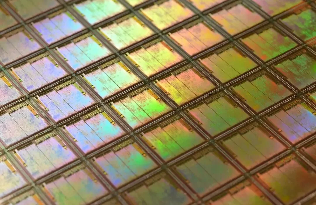
A semiconductor wafer is a thin, circular slice of material-usually silicon. This wafer acts as the base on which electronic circuits are built. Each wafer can hold hundreds or even thousands of individual chips, depending on its size and complexity.
These chips contain tiny electronic components such as transistors, which control the flow of electricity. Once manufacturing is complete, the wafer is cut into individual chips that go on to power:
- phones
- laptops
- servers
- cars
- medical devices
- and more
In simple terms, wafers are the starting point for all modern electronics. Make sure to consult experts to learn more, such as patterned silicon wafers.
Why Precision Matters So Much
Precision is the most important factor in wafer manufacturing. Today’s chips are incredibly complex. A single processor may contain billions of transistors, each smaller than a virus.
If even one part is slightly off, the chip may fail. Precision matters in several key ways:
- Size accuracy
- Material purity
- Surface flatness
Because of these requirements, wafer manufacturing is one of the most advanced engineering processes in the world.
How Wafers Are Made: Step by Step
Before electronic circuits can be built, wafers must go through a carefully controlled manufacturing process that turns raw silicon into a perfectly prepared surface. Each step is designed to achieve extreme purity, accuracy, and consistency, ensuring the wafer is ready for advanced chip fabrication. Here are those steps:
Growing the Silicon Crystal
The process begins with ultra-pure silicon. This silicon is melted at very high temperatures and then slowly cooled to form a single crystal. The most common method used is the Czochralski process.
In this process, a small seed crystal is dipped into molten silicon and slowly pulled upward. As it rises, silicon atoms arrange themselves into a perfectly ordered crystal structure. The result is a large cylindrical block called an ingot.
To give silicon specific electrical properties, tiny amounts of other elements are added. This step, called doping, must be controlled extremely carefully.
Cutting the Ingot into Wafers
Once the silicon ingot is ready, it is sliced into thin wafers using precision diamond saws. Each slice must have:
- A uniform thickness
- Minimal surface damage
- Very tight tolerances
Even small variations can cause problems later during chip manufacturing. Engineers work to reduce material waste while maintaining high accuracy.
Polishing the Wafer Surface
After slicing, wafers are polished until their surfaces are almost perfectly smooth. This is done using chemical mechanical planarization (CMP).
CMP combines chemical solutions with gentle mechanical force to remove tiny surface imperfections. The goal is a mirror-like finish that allows circuit layers to be built evenly.
A wafer that looks smooth to the human eye may still be too rough at the atomic level. That is why polishing must be incredibly precise.
Building Circuits on the Wafer
Once the wafer is ready, actual chip manufacturing begins. This stage is known as fabrication, and it involves building electronic circuits layer by layer.
Photolithography: Printing Tiny Patterns
Photolithography is similar to photography, but on a microscopic scale:
A light-sensitive coating is applied to the wafer. Ultraviolet light shines through a patterned mask.
The pattern is transferred onto the wafer surface. Chemical processes remove or add material to form circuits.
This process is repeated many times. Each cycle adds another layer of components or connections. Modern chips may contain dozens or even hundreds of layers, all perfectly aligned.
Pushing Technology Forward with Precision
For many years, the semiconductor industry followed Moore’s Law, which predicted that the number of transistors on a chip would double every two years. While progress has slowed, precision engineering continues to drive innovation.
Two major advances stand out:
Extreme Ultraviolet (EUV) Lithography
EUV lithography uses extremely short wavelengths of light to create incredibly small features. This allows manufacturers to produce chips with structures smaller than 5 nanometers. EUV systems are among the most complex machines ever built, and they rely on wafers with flawless surfaces.
3D Chip Design
Instead of spreading components across a flat surface, manufacturers now stack layers vertically. This approach improves performance without shrinking every feature.
However, stacking layers increases the need for precise alignment and wafer uniformity. Even tiny errors can multiply across layers.
Next-Generation Technologies Powered by Wafers
Precision-engineered wafers are essential for many advanced technologies shaping the future. Here is the future:
Artificial Intelligence
AI chips must process huge amounts of data quickly. This requires dense circuits and efficient designs that only precision wafers can support.
5G and High-Speed Communication
5G networks depend on chips that operate at very high frequencies. Any variation in wafer quality can reduce signal strength or cause interference.
Electric Vehicles and Power Systems
Electric vehicles rely on power electronics to manage energy efficiently. These systems often use advanced materials like silicon carbide (SiC) or gallium nitride (GaN), which require even more precise manufacturing than silicon.
Quantum Computing
Quantum chips are extremely sensitive to defects. Even tiny material flaws can disrupt quantum behavior. Precision-engineered wafers are essential for building stable, scalable quantum systems.
Measuring Perfection: Quality Control
To maintain precision, manufacturers use advanced inspection tools:
Electron microscopes to detect nanoscale defects. Metrology systems to measure dimensions and thickness. Data analysis tools to monitor consistency.
These systems ensure that every wafer meets strict quality standards before moving to the next step.
Small Wafers, Big Impact
Precision-engineered wafers may be small and invisible to most users, but their impact is enormous. They enable faster computing, smarter machines, cleaner energy, and new scientific discoveries.
As technology continues to advance, the demand for precision will only increase. In many ways, the future of electronics depends on how perfectly we can engineer these thin slices of crystal. Behind every breakthrough device lies a wafer-crafted with care, precision, and cutting-edge engineering.
If you want to read more articles, visit our blog.
Also READ-How Technology is Revolutionizing Patient Engagement